3D Measuring Laser Microscope 예약 안내


- 이용안내
- 연구 장비 예약
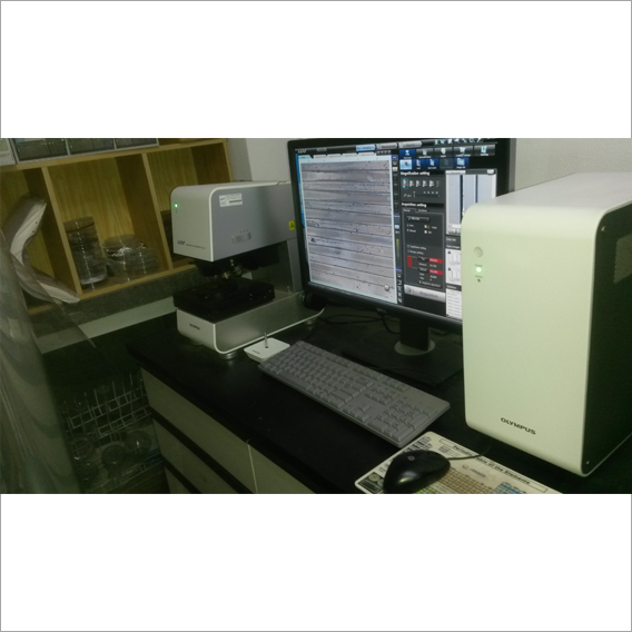
| 연구장비명(영문) | 3D Measuring Laser Microscope |
|---|---|
| 연구장비명(한글) | 3차원 측정 레이저 현미경 |
| 모델명 | OLS4100-SAF |
| 제조회사 | OLYMPUS |
| 도입시기 | 2014.03.13 |
| 보유학과 | 기계공학부 |
| 장비 책임자 | 김석민 교수 |
| 담당 | 김석민 교수 / / smkim@cau.ac.kr |
| 장비위치 | 207동 507호 |
| 예약가능여부 | 예약가능 |


담당자 메모
기기소개
 용도 및 원리
재료 공학/의료/생물학/반도체 등의 광범위한 분야의 시료 측정.
- Semiconductor :IC pattern bump hight defect inspection CMP process
- FPD products :LCD column spacer height coating inspection
- MEMS devices :3D profile of structuresurface roughness MEMS pattern
- Glass surface :Thin film solar cell laser pattering scratch depth - Material Researches :Tooling surface inspection roughness crack analysis
규격 및 사양1. 레이저 관찰부
- 광원 : 405nm 반도체 레이저 / 센터 : Photomultiplier
- Optical Zoom : 1x to 8x(pitch:0.1 for 1x to 2x 1.0 for 2x to 8x)
2. 컬러 관찰부
- 광원 : 백색LED / 센서 : 1/1.8inch 2백만 화소 short plate CCD
- 1x to 8x의 디지털 줌(pitch : 0.1 for 1x to 2x 1.0 for 2x to 8x)
3. Revolving Nosepiece : Motorized 6-position revolving nosepiece
4. 렌즈 ( 5x, 10x, 20x, 50x , 100x )
5. 배율 : 최저 108배 ~ 최고 17280배
6. Image resolution: 4096 x 4096 ~ 1024 x 128
7. 측정 가능 데이터 : 거리측정 선폭측정 단차측정 기하측정 면적 체적 표면적 측정 조도 2D 3D image tiling